| CPC H10B 43/20 (2023.02) [H10B 41/20 (2023.02)] | 31 Claims |

|
1. A process for forming a memory structure above a semiconductor substrate, comprising:
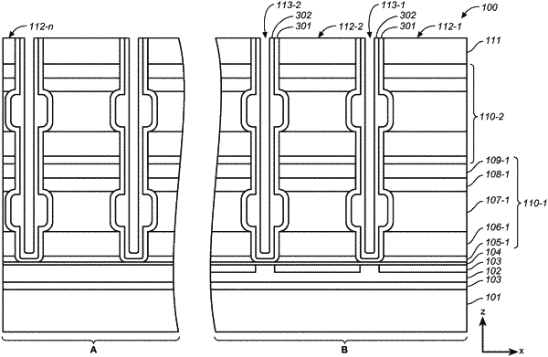
forming a plurality of stacks of semiconductor multi-layers, the semiconductor multilayers within each stack being provided one above another along a first direction substantially orthogonal to the planar surface of the semiconductor substrate and isolated one from another by an isolation layer, each semiconductor multi-layer including (i) first and second semiconductor layers of a first conductivity, and (ii) a dielectric layer provided between the first and second semiconductor layers, each stack being separated from another by one of a first plurality of trenches (“first trenches”), with each first trench running along a second direction substantially parallel to the planar surface of the substrate;
etching recesses into the dielectric layers from their exposed sidewalls facing the first trenches;
depositing conformally a third semiconductor layer over the exposed sidewalls of the stacks in the first trenches;
depositing a covering layer over the third semiconductor layer and filling the recesses;
etching back the covering layer to expose portions of the third semiconductor layer on the sidewalls of the stacks in the first trenches, while retaining, in each recess a portion of the covering layer, so as to prevent a corresponding portion of the third semiconductor layer from being exposed in the first trenches;
removing the exposed portions of the third semiconductor layer; and
filling the first trenches by a filler material.
|