| CPC H10B 10/12 (2023.02) [G11C 11/412 (2013.01); G11C 11/417 (2013.01); H01L 23/5223 (2013.01); H01L 28/56 (2013.01); H01L 28/75 (2013.01); H01L 28/90 (2013.01); H10B 10/00 (2023.02); H10B 10/125 (2023.02)] | 7 Claims |
|
1. A manufacturing method of a static random-access memory device, comprising:
providing a substrate;
forming a first transistor and a second transistor on the substrate, wherein the first transistor comprises a first gate, a first source node, and a first drain node, and the second transistor comprises a second gate, a second source node, and a second drain node;
forming an inner dielectric layer covering the first transistor and the second transistor;
forming a plurality of contacts coupled to the first source node and the second source node in the inner dielectric layer;
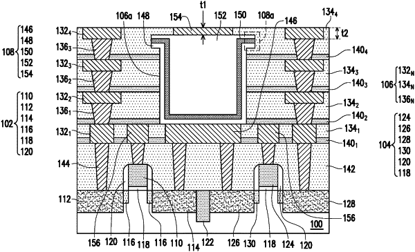
forming a metal interconnect structure on the inner dielectric layer, wherein the metal interconnect structure comprises a plurality of metal layers, a plurality of interlayer dielectric (ILD) layers, and a plurality of vias connected to different layers of the plurality of metal layers, wherein a portion of an n-th metal layer of the plurality of metal layers is utilized as a lower metal layer, wherein n≥1;
forming an opening in the metal interconnect structure, wherein a bottom of the opening exposes the lower metal layer; and
forming a capacitor in the opening, wherein the capacitor comprises the lower metal layer, a first electrode layer formed at a surface of the opening, a dielectric layer formed at a surface of the first electrode layer, a second electrode layer completely filling the opening and covering the dielectric layer, and an upper metal layer formed at a surface of the second electrode layer, and the upper metal layer is a portion of an m-th metal layer of the plurality of metal layers, wherein m≥n+1.
|