| CPC H05K 1/116 (2013.01) [H01L 25/0753 (2013.01); H05K 3/3447 (2013.01); H05K 3/4046 (2013.01); H01L 33/62 (2013.01); H05K 1/18 (2013.01); H05K 2201/09672 (2013.01); H05K 2201/10106 (2013.01); H05K 2201/10287 (2013.01); H05K 2203/0156 (2013.01)] | 21 Claims |
|
1. A substrate structure, comprising:
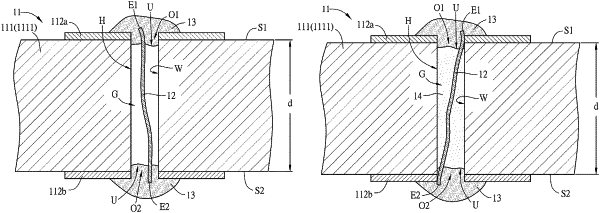
a substrate having a substrate body, a plurality of through holes, a plurality of first conductive pads, and a plurality of second conductive pads, wherein the substrate body is defined with a first surface and a second surface opposite to each other, the through holes penetrate through the substrate body, each of the through holes is defined with a first opening and a second opening opposite to each other, and a hole wall, the first conductive pads are distributed on the first surface of the substrate body and adjacent to the first openings of the through holes, and the second conductive pads are distributed on the second surface of the substrate body and adjacent to the second openings of the through holes;
a plurality of conductive wires arranged in the through holes, wherein each of the conductive wires extends from the first opening to the second opening of the corresponding through hole, each of the conductive wires is defined with a first end and a second end, the first end of the conductive wire is located at the first opening of the corresponding through hole, and the second end of the conductive wire is located at the second opening of the corresponding through hole;
a plurality of conductive members distributed on the first surface and the second surface of the substrate body, wherein the first end of each of the conductive wires is electrically connected to the corresponding first conductive pad through one of the conductive members, and the second end of each of the conductive wires is electrically connected to the corresponding second conductive pad through one of the conductive members; and
a plurality of organic materials;
wherein, at least one part of each of the conductive wires does not contact the hole wall of the corresponding through hole in a direct manner, each of the through holes is defined with a gap between the hole wall and the corresponding conductive wire, each of the organic materials is filled in each of the gaps, and each of the organic materials connects the corresponding conductive wire and the corresponding hole wall.
|