| CPC H05K 1/0222 (2013.01) [H01L 23/50 (2013.01); H01L 23/66 (2013.01); H05K 1/0228 (2013.01); H05K 3/40 (2013.01); H01L 2223/6638 (2013.01)] | 21 Claims |

|
1. An integrated circuit package, comprising:
a printed circuit board having a major plane;
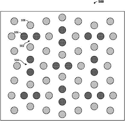
a first plurality of signal pins, each signal pin in the first plurality of signal pins extending in a first direction orthogonal to the major plane, the first plurality of signal pins being grouped into a second plurality of differential signal pin pairs, each differential signal pin pair in the second plurality of differential signal pin pairs being positioned at a vertex of a regular array of orthogonal rows and columns; and
a plurality of ground pins, each ground pin in the plurality of ground pins extending orthogonally to the major plane in the first direction, wherein:
each differential signal pin pair in the second plurality of differential signal pin pairs comprises a positive signal pin and a negative signal pin;
the second plurality of differential signal pin pairs comprises:
a first subset of differential signal pin pairs in which, in each differential signal pin pair, the positive signal pin and the negative signal pin are arranged relative to one another in a first orientation along a line parallel to rows of the array; and
a second subset of differential signal pin pairs in which, in each differential signal pin pair, the positive signal pin and the negative signal pin are arranged relative to one another in a second orientation along a line parallel to columns of the array;
for each differential signal pin pair in one of the first and second subsets, all nearest neighbor differential signal pin pairs belong to another of the first and second subsets; and
at least one ground pin of the plurality of ground pins is arranged between a first differential signal pin pair and a second differential signal pin pair, the at least one ground pin being disposed (a) along a line connecting a first vertex of the regular array of rows and columns at which the first differential signal pin pair is located to a second vertex of the regular array of rows and columns at which the second differential signal pin pair is located, and (b) along a line connecting a first differential signal pin in the first differential signal pin pair to a first differential signal pin in the second differential signal pin pair, and (c) along a line connecting a second differential signal pin in the first differential signal pin pair to a second differential signal pin in the second differential signal pin pair, to shield at least one differential signal pin in the first differential signal pin pair from signals in the second differential signal pin pair, or to shield at least one differential signal pin in the second differential signal pin pair from signals in the first differential signal pin pair.
|