| CPC H03F 1/0288 (2013.01) [H03F 3/211 (2013.01); H03K 5/01 (2013.01); H05K 1/0243 (2013.01); H03F 2200/451 (2013.01); H03K 2005/00078 (2013.01)] | 4 Claims |

|
1. A high frequency amplifier comprising:
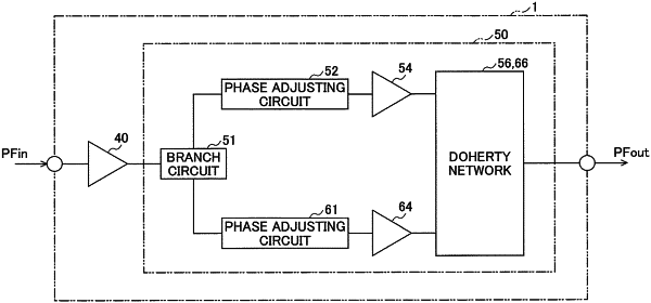
an asymmetrical Doherty amplifier that includes a carrier amplifier, a peak amplifier, a branch circuit, and a phase adjusting circuit, and is configured to amplify an input high frequency signal;
a driver amplifier configured to drive the asymmetrical Doherty amplifier;
a first circuit board mounting the driver amplifier, the carrier amplifier, and the peak amplifier;
a second circuit board mounting the branch circuit and the phase adjusting circuit; and
a base member mounting the first circuit board and the second circuit board,
wherein the peak amplifier has a saturation output different from a saturation output of the carrier amplifier and is configured to initiate an amplifying operation when an output of the carrier amplifier reaches a saturation region,
the branch circuit is configured to divide a path of a high frequency signal amplified by the driver amplifier into input paths of the peak amplifier and the carrier amplifier,
the phase adjusting circuit is provided on at least one of the input paths of the peak amplifier and the carrier amplifier to delay at least one of phases of input signals of the peak amplifier and the carrier amplifier,
the driver amplifier, the carrier amplifier, and the peak amplifier each include a front surface having a circuit thereon and a rear surface opposite to the front surface,
each of the rear surfaces of the driver amplifier, the carrier amplifier, and the peak amplifier is in contact with the base member,
the second circuit board is stacked on the first circuit board,
an input terminal of the driver amplifier and an input terminal of the peak amplifier are adjacent to each other, and
an electrical length from an output terminal of the driver amplifier to the input terminal of the peak amplifier, when converted based on a phase of the input high frequency signal, is from (2n+1)×π−π/4 to (2n+1)×π+π/4, where n is an integer greater than or equal to zero.
|