| CPC H02M 3/1586 (2021.05) [H02M 1/0009 (2021.05); H02M 1/0083 (2021.05)] | 12 Claims |

|
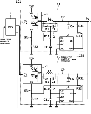
1. A power supply system comprising:
a plurality of power conversion circuits, each including an inductor connected in series to a current path configured to supply a current to an output;
a switching element configured to generate a switching current flowing through the inductor;
an individual current detection circuit provided for each of the power conversion circuits and configured to generate an inductor current signal proportional to a magnitude of a current flowing through the inductor;
an integrated individual current balance circuit provided for each of the power conversion circuits and having at least a current signal terminal, a common node terminal, and a feedback signal adjustment terminal;
an integrated individual switching control circuit provided for each of the power conversion circuits, having a feedback terminal that inputs at least a feedback signal, and configured to generate a control signal for the switching element;
a common output portion configured to merge output currents of the plurality of power conversion circuits; and
a current sharing signal line that connects the common node terminals of the plurality of power conversion circuits,
wherein
the individual current balance circuit is configured to output the inductor current signal input to the current signal terminal to the common node terminal and generate an individual feedback signal output to the feedback signal adjustment terminal according to the inductor current signal and a voltage of the common node terminal, and
the individual switching control circuit is configured to equalize currents flowing through respective inductors of the plurality of power conversion circuits by controlling the switching element in accordance with the individual feedback signal input to the feedback terminal, and controls a voltage of the common output portion to a constant voltage value to be stabilized.
|