| CPC H02M 3/003 (2021.05) [H02M 1/0006 (2021.05); H02M 1/0095 (2021.05); H02M 3/158 (2013.01)] | 20 Claims |
|
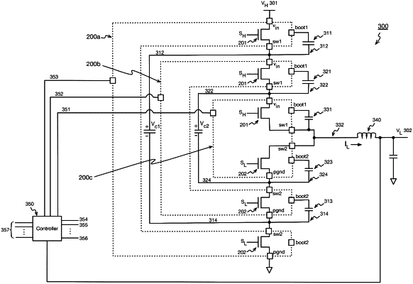
1. An apparatus, comprising:
a multi-level power converter including a plurality of power semiconductor packages, wherein the plurality of power semiconductor packages individually comprise:
a power transfer path comprising at least a high-side switch and a low-side switch each comprising a vertical field effect transistor including a first node and a second node arranged vertically with respect to each other along a direction perpendicular to a major surface of an individual power semiconductor package;
a first terminal coupled to the first node of the high-side switch;
a second terminal coupled to the second node of the low-side switch;
a high-side switch terminal coupled to the second node of the high-side switch; and
a low-side switch terminal coupled to the first node of the low-side switch,
wherein the high-side switch terminal and the low-side switch terminal comprise separate terminals, and
at least one of the first terminal or the second terminal includes terminal lead frame contacts arranged along an edge of the individual power semiconductor package.
|