US 11,916,285 B2
Wiring board and method for manufacturing wiring board
Koichi Suzuki, Tokyo (JP); Seiji Take, Tokyo (JP); and Daisuke Matsuura, Tokyo (JP)
Assigned to Dai Nippon Printing Co., Ltd., Tokyo (JP)
Appl. No. 17/280,279
Filed by Dai Nippon Printing Co., Ltd., Tokyo (JP)
PCT Filed Sep. 19, 2019, PCT No. PCT/JP2019/036679
§ 371(c)(1), (2) Date Mar. 26, 2021,
PCT Pub. No. WO2020/066817, PCT Pub. Date Apr. 2, 2020.
Claims priority of application No. 2018-186161 (JP), filed on Sep. 28, 2018.
Prior Publication US 2022/0037777 A1, Feb. 3, 2022
Int. Cl. H05K 1/09 (2006.01); H05K 3/10 (2006.01); H01Q 1/38 (2006.01); H05K 1/02 (2006.01)
CPC H01Q 1/38 (2013.01) [H05K 1/0274 (2013.01); H05K 1/0296 (2013.01); H05K 1/09 (2013.01); H05K 3/10 (2013.01); H05K 2201/10098 (2013.01)] 12 Claims
OG exemplary drawing
 
1. A wiring board comprising:
a substrate that is transparent; and
a wiring pattern region that is disposed on the substrate and that includes a plurality of wiring lines,
wherein the wiring pattern region has a sheet resistance of less than or equal to 5 Ω/sq, and
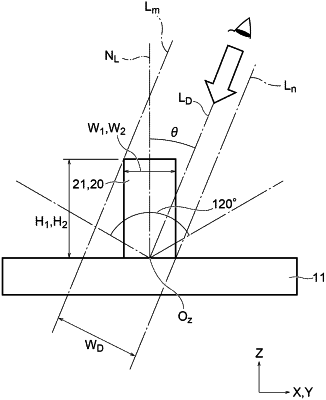
wherein each wiring line has a maximum width of less than or equal to 3 μm when viewed at a viewing angle of 120°.