| CPC H01L 33/504 (2013.01) [H01L 33/502 (2013.01); H01L 33/505 (2013.01); H01L 33/507 (2013.01); H01L 33/58 (2013.01); H01L 33/644 (2013.01)] | 19 Claims |

|
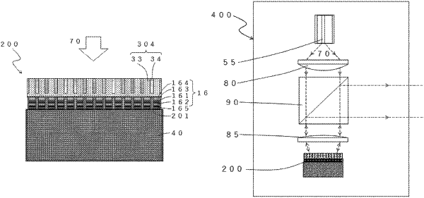
1. A wavelength conversion component comprising:
a plurality of semiconductor multilayer film segments;
a first member arranged between adjacent ones of the semiconductor multilayer film segments; and
a substrate disposed above the plurality of semiconductor multilayer film segments, the substrate defining a groove, wherein
each of the semiconductor multilayer film segments is configured to receive light, convert a wavelength of the light received, and allow a wavelength-converted light to exit toward the substrate.
|