| CPC H01L 33/32 (2013.01) [H01L 27/156 (2013.01); H01L 33/0075 (2013.01); H01L 33/62 (2013.01); H01L 2933/0066 (2013.01)] | 24 Claims |

|
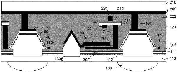
1. An active matrix LED array precursor comprising:
a common first semiconducting layer comprising a substantially undoped Group III-nitride;
a plurality of transistor-driven LED precursors, each transistor-driven LED precursor comprising:
a monolithic light emitting diode (LED) structure comprising a plurality of III-nitride semiconducting layers, each monolithic LED structure formed on a portion of the common semiconducting layer;
a barrier semiconducting layer formed on a portion of the common semiconducting layer encircling the LED structure configured to induce a two-dimensional electron channel layer at the interface between the common semiconducting layer and the barrier semiconducting layer; and
a gate contact formed over a portion of the two-dimensional electron channel layer, the gate contact encircling the LED structure; and
a common source contact configured to form an ohmic contact to each two-dimensional electron channel layer such that a high electron mobility transistor is provided between the common source contact and each monolithic LED structure for driving each LED structure.
|