| CPC H01L 33/08 (2013.01) [H01L 25/0753 (2013.01); H01L 33/405 (2013.01); H01L 33/46 (2013.01); H01L 2224/32257 (2013.01); H01L 2224/48091 (2013.01); H01L 2224/48247 (2013.01); H01L 2224/73265 (2013.01)] | 13 Claims |
|
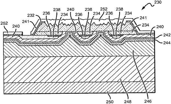
1. A method for fabricating a lighting device, the method comprising:
separating a plurality of LED active regions of a wafer, wherein LED active regions of the plurality of LED active regions are supported by a structure including one or more insulating material layers, including electrically conductive interconnect elements embedded within said one or more insulating material layers, and a plurality of electrically conductive vias extending from the electrically conductive interconnect elements to contact the plurality of LED active regions, wherein the electrically conductive interconnect elements and the plurality of electrically conductive vias connect at least some LED active regions of the plurality of LED active regions in series, in parallel, or in series-parallel; and
mounting the structure to a submount, with the one or more insulating material layers arranged between the submount and the plurality of LED active regions;
wherein the plurality of electrically conductive vias includes a first group of one or more electrically conductive vias coupled with an n-type layer of the plurality of LED active regions, and a second group of one or more electrically conductive vias coupled with a p-type layer of the plurality of LED active regions; and
wherein each electrically conductive via of the first group of one or more electrically conductive vias comprises a greater height than each electrically conductive via of the second group of one or more electrically conductive vias.
|