US 11,916,154 B2
Light receiving element and ranging module having a plurality of pixels that each includes voltage application units and charge detection units
Koji Neya, Kanagawa (JP); and Takuya Maruyama, Kanagawa (JP)
Assigned to Sony Semiconductor Solutions Corporation, Kanagawa (JP)
Filed by SONY SEMICONDUCTOR SOLUTIONS CORPORATION, Kanagawa (JP)
Filed on Dec. 27, 2022, as Appl. No. 18/089,293.
Application 18/089,293 is a continuation of application No. 16/633,710, granted, now 11,538,942, previously published as PCT/JP2019/026576, filed on Jul. 4, 2019.
Claims priority of application No. 2018-135352 (JP), filed on Jul. 18, 2018.
Prior Publication US 2023/0137903 A1, May 4, 2023
This patent is subject to a terminal disclaimer.
Int. Cl. H01L 31/02 (2006.01); G01S 7/4863 (2020.01); H01L 31/0216 (2014.01); H01L 31/103 (2006.01)
CPC H01L 31/02019 (2013.01) [G01S 7/4863 (2013.01); H01L 31/02164 (2013.01); H01L 31/103 (2013.01)] 24 Claims
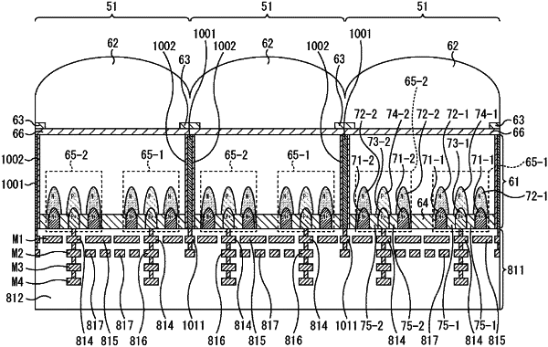
OG exemplary drawing
 
1. A light receiving element, comprising:
a plurality of pixels, each including:
a first voltage application unit to which a first voltage is applied;
a first charge detection unit provided adjacent to the first voltage application unit;
a second voltage application unit to which a second voltage different from the first voltage is applied; and
a second charge detection unit provided adjacent to the second voltage application unit; and
a trench that is arranged between the pixels adjacent to each other in a semiconductor layer.