| CPC H01L 29/7813 (2013.01) [H01L 29/0623 (2013.01); H01L 29/407 (2013.01); H01L 29/66734 (2013.01)] | 5 Claims |
|
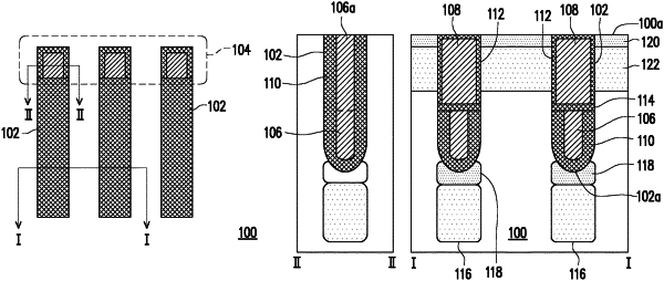
1. A method for fabricating a shield gate MOSFET, comprising:
forming an epitaxial layer, wherein the epitaxial layer has a first conductivity type;
forming a plurality of trenches in the epitaxial layer, wherein a connecting region is defined in one end of each of the trenches;
forming a first doped region and a second doped region in the epitaxial layer at a bottom of each of the trenches, wherein the first doped region has a second conductivity type, and the second doped region has the first conductivity type;
forming an insulating layer on a surface of the epitaxial layer in each of the trenches;
forming a conductive layer on the insulating layer in each of the trenches;
forming a protective layer on the connecting region;
removing a portion of the conductive layer except for the connection region to form a shield gate, expose a portion of the insulating layer, and keep the conductive layer in the connection region;
removing the exposed portion of the insulating layer and expose a portion of the epitaxial layer in the trenches;
removing the protective layer;
rounding a top surface of the shield gate and a top surface of the conductive layer in the connecting region;
forming an inter-gate oxide layer and a gate oxide layer in the trenches, wherein the inter-gate oxide layer covers the rounded top surface of the shield gate, and the gate oxide layer covers a surface of the exposed portion of the epitaxial layer, wherein the inter-gate oxide layer or the gate oxide layer covers the rounded top surface of the conductive layer in the connecting region; and
forming a control gate on the inter-gate oxide layer in the plurality of trenches.
|