| CPC H01L 29/7455 (2013.01) [H01L 29/66363 (2013.01); H01L 29/7424 (2013.01)] | 12 Claims |
|
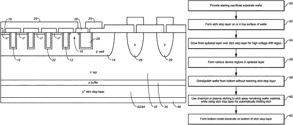
1. A method for forming a vertical power device comprising:
providing a silicon substrate wafer having a top surface and a bottom surface;
forming a silicon p− type etch stop layer over or in the top surface of the wafer, the etch stop layer having an etch rate, when using a first type of etchant material, lower than the etch rate of the wafer underlying the etch stop layer, wherein the etch rate of the etch stop layer is determined by a p− type dopant concentration in the etch stop layer, the etch stop layer being conductive;
epitaxially growing a drift layer overlying the etch stop layer;
forming one or more doped regions in or over the drift layer;
etching at least a portion of the wafer, using the first type of etchant material, to remove the wafer while retaining the etch stop layer such that the etch stop layer has an exposed surface, the etch stop layer automatically reducing the etch rate; and
forming a metal electrode on the exposed surface of the etch stop layer, whereby, when the device is turned on and conducting a vertical current, the current flows through the metal electrode and the etch stop layer.
|