| CPC H01L 29/66924 (2013.01) [H01L 21/0254 (2013.01); H01L 21/02639 (2013.01); H01L 21/308 (2013.01); H01L 21/30612 (2013.01); H01L 29/2003 (2013.01); H01L 29/66909 (2013.01); H01L 29/8083 (2013.01)] | 20 Claims |
|
1. A semiconductor device comprising:
a semiconductor substrate having a first conductivity type;
a drift layer of the first conductivity type coupled to the semiconductor substrate;
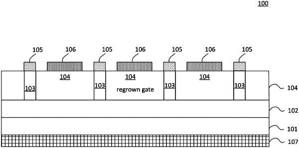
a fin array comprising a plurality of rows of fins on the drift layer, the plurality of rows of fins including a first row of fins and a second row of fins, the first row of fins comprising a plurality of first elongated fins arranged in parallel to each other along a first row direction and separated by a first distance, and the second row of fins comprising a plurality of second elongated fins arranged in parallel to each other along a second row direction and separated by a second distance equal to the first distance;
a gate layer of a second conductivity type opposite the first conductivity type on the drift layer and surrounding each of the plurality of first elongated fins and each of the plurality of second elongated fins; and
a space equal to the first distance between the first row of fins and the second row of fins.
|