| CPC H01L 29/66151 (2013.01) [B82Y 10/00 (2013.01); H01L 21/28 (2013.01); H01L 21/283 (2013.01); H01L 29/068 (2013.01); H01L 29/0665 (2013.01); H01L 29/0673 (2013.01); H01L 29/0676 (2013.01); H01L 29/08 (2013.01); H01L 29/417 (2013.01); H01L 29/66143 (2013.01); H01L 29/872 (2013.01); H01L 29/88 (2013.01); H10N 70/00 (2023.02); H01L 28/90 (2013.01)] | 10 Claims |

|
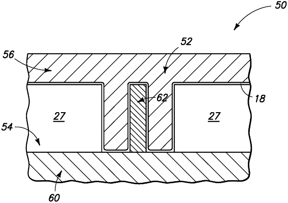
6. A method for forming a diode construction, the method comprising:
forming insulative material over a base;
patterning the insulative material to form a first opening extending through the insulative material to the base;
forming spacer material within opening;
patterning the spacer material into a pair of spacers defining a second opening having width in at least one cross section narrower than a width of the first opening;
forming electrically conductive material within the second opening, upon the base, and between the spacers;
removing the spacers to form third and fourth openings about the electrically conductive material;
depositing one or more layers within the third and fourth openings and over the insulative material, over the base, and over the electrically conductive material to form an intermediate diode structure, wherein the intermediate diode structure consists essentially of one or more of aluminum nitride, aluminum oxide, hafnium oxide, magnesium oxide, niobium oxide, silicon nitride, silicon oxide, tantalum oxide, titanium oxide, yttrium oxide, and/or zirconium oxide; and
forming an electrode over the intermediate diode structure to formation of the diode construction.
|