US 11,916,118 B2
Stacked source-drain-gate connection and process for forming such
Ehren Mannebach, Beaverton, OR (US); Aaron Lilak, Beaverton, OR (US); Hui Jae Yoo, Portland, OR (US); Patrick Morrow, Portland, OR (US); Anh Phan, Beaverton, OR (US); Willy Rachmady, Beaverton, OR (US); Cheng-Ying Huang, Portland, OR (US); and Gilbert Dewey, Beaverton, OR (US)
Assigned to Intel Corporation, Santa Clara, CA (US)
Filed by Intel Corporation, Santa Clara, CA (US)
Filed on Apr. 4, 2023, as Appl. No. 18/130,824.
Application 18/130,824 is a continuation of application No. 16/455,669, filed on Jun. 27, 2019, granted, now 11,646,352.
Prior Publication US 2023/0238436 A1, Jul. 27, 2023
Int. Cl. H01L 29/417 (2006.01)
CPC H01L 29/41741 (2013.01) [H01L 29/41775 (2013.01)] 20 Claims
OG exemplary drawing
 
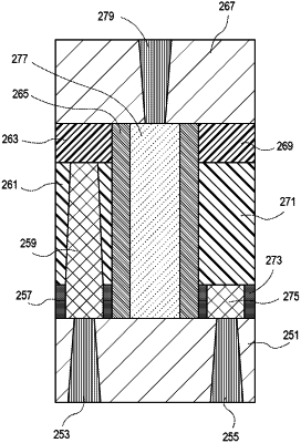
1. An integrated circuit structure, comprising:
a fin having a channel region;
a gate structure over the channel region of the fin, the gate structure comprising a first gate electrode, and a second gate electrode vertically over the first gate electrode;
a source or drain structure laterally spaced apart from the gate structure;
a first conductive via beneath the gate structure, the first conductive via in contact with the first gate electrode; and
a second conductive via above the source or drain structure and laterally spaced apart from the gate structure, the second conductive via in contact with the source or drain structure.