| CPC H01L 29/1604 (2013.01) [H01L 21/0254 (2013.01); H01L 21/0259 (2013.01); H01L 21/02428 (2013.01); H01L 21/02488 (2013.01); H01L 21/02546 (2013.01); H01L 21/02617 (2013.01); H01L 29/04 (2013.01)] | 7 Claims |

|
1. A method of fabricating a single crystal semiconductor structure, the method comprising:
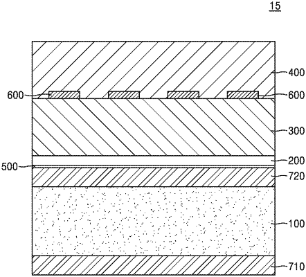
forming an orienting thin film on an amorphous substrate;
forming a lower single crystal layer on the orienting thin film;
forming an upper single crystal layer on the lower single crystal layer; and
forming a mask pattern between the lower single crystal layer and the upper single crystal layer,
wherein the orienting thin film has a non-zero thickness that is equal to or less than 10 times a critical thickness hc,
wherein the critical thickness hc is determined by the following equation:
 where b is a Burgers vector of dislocation of the orienting thin film, μ is Poisson's ratio of the orienting thin film, and ε0 is a degree of lattice misfit between the orienting thin film and the lower single crystal layer,
wherein the lower single crystal layer and the upper single crystal layer each comprise a Group III-V compound semiconductor layer,
wherein the mask pattern comprises holes through which the lower single crystal layer is exposed to the upper single crystal layer, and
wherein the upper single crystal layer is formed to fill the holes and cover a top surface of the mask pattern.
|