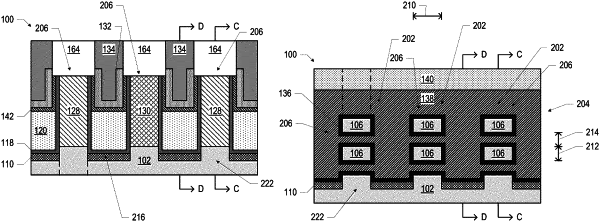
| CPC H01L 29/0653 (2013.01) [H01L 24/43 (2013.01); H01L 2924/14 (2013.01)] | 27 Claims |

|
1. An integrated circuit (IC) device, comprising:
a first channel region of a first transistor and an adjacent second channel region of a second transistor;
a first region proximate to the first channel region;
a second region proximate to the second channel region, wherein one of the first region and the second region is one of a source region and a drain region and another one of the first region and the second region is another one of the source region and the drain region; and
an insulating material region at least partially between the first region and the second region, wherein the insulating material region includes a first insulating material and a second insulating material, wherein the first insulating material has a U-shaped cross-section, and the first insulating material is between the second insulating material and the first region.
|