| CPC H01L 27/124 (2013.01) [G06V 40/1318 (2022.01); H01L 25/167 (2013.01); H01L 25/18 (2013.01); H01L 27/14678 (2013.01); H01L 27/156 (2013.01); H10K 59/123 (2023.02); H10K 59/126 (2023.02); H10K 59/65 (2023.02)] | 20 Claims |

|
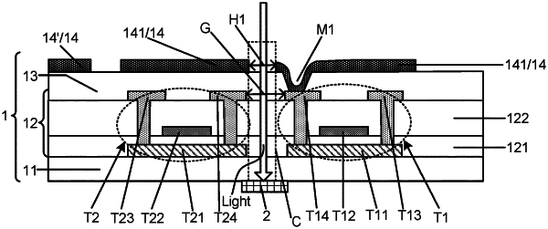
1. A display substrate having an active area, the active area including a photosensitive region having a light-transmitting channel, the display substrate comprising:
a base;
a pixel circuit layer disposed on the base, the pixel circuit layer including a plurality of pixel circuits located in the active area, and at least one pixel circuit including a first thin film transistor and a second thin film transistor;
a first insulating layer disposed on a side of the pixel circuit layer away from the base, the first insulating layer having a first via hole; and
a conductive light-shielding layer disposed on a side of the first insulating layer away from the base, wherein
the conductive light-shielding layer includes a conductive light-shielding pattern that has a first light-transmitting hole located in the photosensitive region; an orthogonal projection of the first light-transmitting hole on the base and an orthogonal projection of a gap region between the first thin film transistor and the second thin film transistor on the base have a first overlapping region, the light-transmitting channel is perpendicular to the base and penetrates the first overlapping region;
the conductive light-shielding pattern is coupled with a source electrode or a drain electrode of the first thin film transistor through the first via hole.
|