| CPC H01L 27/124 (2013.01) [H01L 27/127 (2013.01); H01L 27/1225 (2013.01); H01L 27/1229 (2013.01); H01L 27/1248 (2013.01); H01L 27/1251 (2013.01)] | 4 Claims |
|
1. A method of manufacturing an array substrate, comprising following steps:
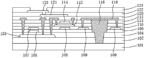
step S1, forming an inorganic stacked layer and a plurality of first metal lines on a substrate layer, wherein the substrate layer comprises a bending area and a non-bending area, the first metal lines are disposed in the non-bending area at two sides of the bending area and are embedded in the inorganic stacked layer;
step S2, patterning the inorganic stacked layer to form a recess in the bending area;
step S3, filling the recess with a filling layer; and
step S4, forming a source/drain metal layer on the inorganic stacked layer and the filling layer, and patterning the source/drain metal layer to form a second metal line in the bending area, wherein the second metal line and the first metal lines disposed at the two sides of the bending area form a lap joint;
wherein the step S1 comprises following steps:
step 101, sequentially forming a first active layer, a first gate insulating layer, a first gate corresponding to the first active layer, and a second gate insulating layer on the substrate layer;
step 102, forming a first electrode layer on the second gate insulating layer, patterning the first electrode layer to form a first electrode corresponding to the first gate, a second electrode spaced apart from the first electrode, and the first metal lines disposed at the two sides of the bending area; and
step 103, sequentially forming a first dielectric layer, a second active layer corresponding to the second electrode, a third gate insulating layer, a second gate corresponding to the second active layer, and a second dielectric layer on the first electrode;
wherein the inorganic stacked layer comprises a buffer layer, the first gate insulating layer, the second gate insulating layer, the first dielectric layer, the third gate insulating layer, and the second dielectric layer, which are stacked;
wherein the step of patterning the inorganic stacked layer comprises following steps:
step S201, etching the inorganic stacked layer for a first time to form a plurality of first openings corresponding to two ends of the second active layer and penetrating the second dielectric layer and the third gate insulating layer;
step S202, etching the inorganic stacked layer for a second time to form a plurality of second openings corresponding to the first metal lines and a plurality of third openings corresponding to two ends of the first active layer, wherein the second openings penetrate the second dielectric layer, the third gate insulating layer, and the first dielectric layer, and the third openings penetrate the second dielectric layer, the third gate insulating layer, the first dielectric layer, the second gate insulating layer, and the first gate insulating layer;
step S203, etching the inorganic stacked layer for a third time to form a fourth opening corresponding to the bending area and penetrating the second gate insulating layer, the first dielectric layer, the third gate insulating layer, and the second dielectric layer; and
step S204, etching the inorganic stacked layer for a fourth time to form a fifth opening corresponding to the bending area and penetrating the buffer layer and the first gate insulating layer, wherein the fifth opening and the fourth opening are connected to each other to form the recess.
|