| CPC H01L 27/1207 (2013.01) [H01L 21/823431 (2013.01); H01L 21/823437 (2013.01); H01L 21/823456 (2013.01); H01L 21/823487 (2013.01); H01L 21/84 (2013.01); H01L 27/0886 (2013.01); H01L 29/0843 (2013.01); H01L 29/41733 (2013.01); H01L 29/41791 (2013.01); H01L 29/4236 (2013.01); H01L 29/42392 (2013.01); H01L 29/7831 (2013.01); H01L 29/785 (2013.01); H01L 29/78642 (2013.01); H01L 29/78696 (2013.01)] | 20 Claims |

|
1. A semiconductor device comprising:
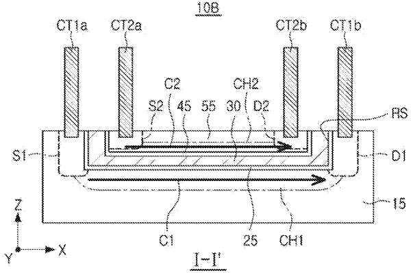
a substrate having an active region defined by a device isolation film, the active region providing a first channel region;
a first source/drain region in the active region on first and second sides of the first channel region;
a gate structure having a first gate insulating film, a shared gate electrode, and a second gate insulating film sequentially arranged on the active region, the shared gate electrode having an extended portion on the device isolation film;
a cover semiconductor layer on the second gate insulating film and electrically separated from the active region to provide a second channel region;
a second source/drain region in the cover semiconductor layer on first and second sides of the second channel region;
first and second source/drain contacts respectively connected to the first and second source/drain regions; and
a shared gate contact connected to the extended portion of the shared gate electrode.
|