| CPC H01L 27/092 (2013.01) [H03K 17/6872 (2013.01)] | 20 Claims |
|
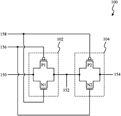
1. A dual transmission gate, comprising:
a first pair of complementary metal-oxide-semiconductor field-effect (CMOS) transistors that is arranged to form a first transmission gate, the first transmission gate being configured to route a first signal between a first terminal and a second terminal in response to a first clocking signal being at a first logical level and a second clocking signal being at a second logical level, the first pair of CMOS transistors including a first p-type metal-oxide-semiconductor field-effect (PMOS) transistor that is situated along a first column or a second column from among a plurality of columns of an electronic device design real estate and a first n-type metal-oxide-semiconductor field-effect (NMOS) transistor that is situated along the first column or the second column;
a second pair of CMOS transistors that is arranged to form a second transmission gate, the second transmission gate being configured to route a second signal between the second terminal and a third terminal in response to the first clocking signal being at the second logical level and the second clocking signal being at the first logical level, the second pair of CMOS transistors including a second PMOS transistor that is situated along the first column or the second column and a second NMOS transistor that is situated along the first column or the second column;
a first region, corresponding to the first clocking signal, situated along a first interconnection layer of a semiconductor stack along a first row from among a plurality of rows of the electronic device design real estate, the first region being connected to the first PMOS transistor and the second NMOS transistor;
a second region, corresponding to the first terminal, situated along the first interconnection layer along a second row from among the plurality of rows of the electronic device design real estate and connected to the first PMOS transistor and the first NMOS transistor;
a third region, corresponding to the second terminal, situated along a second interconnection layer of the semiconductor stack along a second column from among the plurality of columns and connected to the first pair of CMOS transistors and the second pair of CMOS transistors;
a fourth region, corresponding to the second clocking signal, situated along the first interconnection layer along a third row from among the plurality of rows of the electronic device design real estate and connected to the first NMOS transistor and the second PMOS transistor; and
a fifth region, corresponding to the third terminal, situated along the first interconnection layer along a fourth row from among the plurality of rows of the electronic device design real estate and connected to the second PMOS transistor and the second NMOS transistor.
|