| CPC H01L 27/092 (2013.01) [H01L 21/8221 (2013.01); H01L 21/823814 (2013.01); H01L 27/0688 (2013.01); H01L 29/0665 (2013.01); H01L 29/41725 (2013.01); H01L 29/42392 (2013.01); H01L 29/775 (2013.01); H01L 29/78696 (2013.01)] | 12 Claims |

|
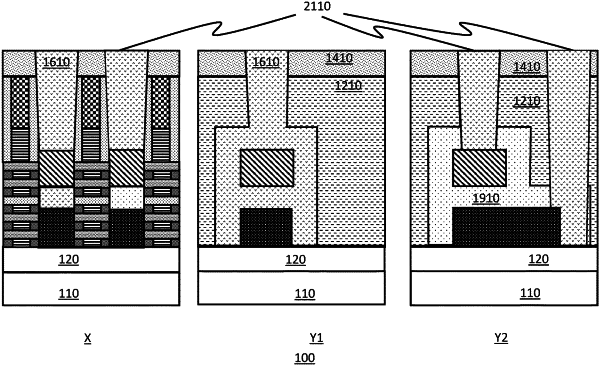
1. A complementary field effect transistor (CFET) structure comprising:
a first transistor disposed above a second transistor;
a first source/drain region of the first transistor disposed above a second source/drain region of the second transistor, wherein the first source/drain region comprises a smaller cross-section than the second source/drain region;
a first dielectric material disposed in contact with a bottom surface and vertical surfaces of the first source/drain and further in contact with a vertical surface and top surface of the second source/drain region;
a second dielectric material disposed as an interlayer dielectric material encapsulating the first transistor and the second transistor;
a third source/drain region of the first transistor disposed above a fourth source/drain region of the second transistor; and
a first metal contact disposed around and in contact with each of the third source/drain region and fourth source/drain region.
|