| CPC H01L 27/0248 (2013.01) [H01L 21/78 (2013.01); H01L 23/5386 (2013.01); H01L 23/5389 (2013.01); H01L 23/60 (2013.01); H01L 24/19 (2013.01); H01L 24/20 (2013.01); H01L 24/97 (2013.01); H01L 25/072 (2013.01); H01L 25/50 (2013.01); H01L 27/0255 (2013.01); H01L 27/0262 (2013.01); H01L 27/0292 (2013.01); H01L 29/7416 (2013.01); H02H 9/04 (2013.01); H01L 27/0744 (2013.01); H01L 29/74 (2013.01); H01L 2224/214 (2013.01); H01L 2224/95001 (2013.01); H01L 2924/1203 (2013.01); H01L 2924/1301 (2013.01); H01L 2924/30205 (2013.01)] | 18 Claims |
|
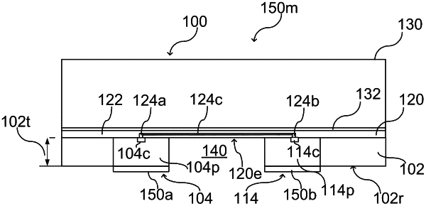
1. An electrostatic discharge protection device comprising:
a first vertically integrated electrostatic discharge protection structure comprising a first semiconductor portion, a first contact region disposed on a first side of the first semiconductor portion and a first terminal exposed on a second side of the first semiconductor portion opposite the first side of the first semiconductor portion;
a second vertically integrated electrostatic discharge protection structure comprising a second semiconductor portion, a second contact region disposed on a first side of the second semiconductor portion and a second terminal exposed on a second side of the second semiconductor portion opposite the first side of the second semiconductor portion;
an electrical connection layer, wherein the first vertically integrated electrostatic discharge protection structure and the second vertically integrated electrostatic discharge protection structure are disposed on the electrical connection layer laterally separated from each other and are electrically connected with each other via the electrical connection layer;
wherein the electrical connection layer is mounted on a support carrier.
|