| CPC H01L 25/167 (2013.01) [H01L 27/1259 (2013.01); H01L 24/05 (2013.01); H01L 27/124 (2013.01); H01L 2224/0568 (2013.01); H01L 2224/05572 (2013.01); H01L 2224/05573 (2013.01); H01L 2224/05624 (2013.01); H01L 2224/05647 (2013.01)] | 13 Claims |

|
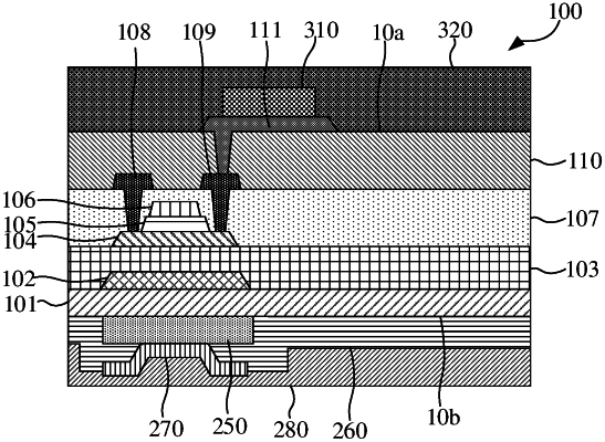
1. A method of manufacturing a display device, comprising the following steps:
step A: forming a thin-film transistor array substrate, the thin-film transistor array substrate comprising a first surface and a second surface that are disposed opposite to each other;
step B: forming a protective layer on the first surface of the thin-film transistor array substrate;
step C: forming a metal layer on the second surface of the thin-film transistor array substrate by a first patterning;
step D: forming a metal member by performing a second patterning on the metal layer;
step E: forming a patterned insulating layer on the second surface of the thin-film transistor array substrate, the patterned insulating layer covering at least a part of the metal member;
step F: forming an electrode layer on the metal member;
step G: forming a planarization layer on the electrode layer and the patterned insulating layer;
step H: removing the protective layer;
step I: disposing a light emitting diode (LED) chip on the first surface of the thin-film transistor array substrate; and
step J: disposing an optical film on the LED chip.
|