| CPC H01L 24/73 (2013.01) [H01L 24/19 (2013.01); H01L 24/20 (2013.01); H01L 24/26 (2013.01); H01L 24/96 (2013.01); H01L 25/0652 (2013.01); H01L 25/18 (2013.01); H01L 25/50 (2013.01); H01L 23/481 (2013.01); H01L 24/16 (2013.01); H01L 24/24 (2013.01); H01L 24/32 (2013.01); H01L 2224/16145 (2013.01); H01L 2224/2101 (2013.01); H01L 2224/221 (2013.01); H01L 2224/24146 (2013.01); H01L 2224/26145 (2013.01); H01L 2224/32145 (2013.01); H01L 2224/73204 (2013.01); H01L 2224/73209 (2013.01); H01L 2224/73217 (2013.01)] | 18 Claims |
|
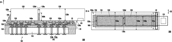
1. A packaging structure, comprising:
a first die, comprising a silicon substrate and a through silicon conductor penetrating the silicon substrate;
an encapsulant, covering the first die;
a redistribution circuit structure, located on the encapsulant;
a second die, disposed on the redistribution circuit structure and electrically connected to the redistribution circuit structure;
a third die, disposed on the redistribution circuit structure and electrically connected to the redistribution circuit structure, wherein the third die has an optical signal transmission area; and
a filler, located between the second die and the redistribution circuit structure and between the third die and the redistribution circuit structure, wherein:
a groove is present on an upper surface of the redistribution circuit structure, and the upper surface comprises a first area and a second area located on opposite sides of the groove;
the filler directly contacts the first area;
the filler is away from the second area; and
the redistribution circuit structure is located on an encapsulant surface of the encapsulant, and in a direction perpendicular to the encapsulant surface, the optical signal transmission area of the third die does not overlap at least two of the filler, the redistribution circuit structure, and the encapsulant.
|