| CPC H01L 23/5226 (2013.01) [H10B 41/10 (2023.02); H10B 41/27 (2023.02); H10B 43/10 (2023.02); H10B 43/27 (2023.02)] | 23 Claims |

|
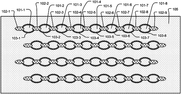
1. A vertical memory structure, comprising:
a stack of alternating layers of insulator material and word line material;
a series of alternating conductive pillars and insulating pillars disposed through stack, the series including at least a first conductive pillar, a first insulating pillar adjacent to the first conductive pillar and a second conductive pillar adjacent to the first insulating pillar, wherein an outside surface of the first insulating pillar is arcuate in a plane parallel to the layers of word line material;
data storage structures disposed on inside surfaces of the layers of word line material at cross-points of the first insulating pillar and the layers of word line material; and
semiconductor channel material between the first insulating pillar and the data storage structures at cross-points of the first insulating pillar with the layers of word line material, the semiconductor channel material extending around an outside surface of the first insulating pillar and directly contacting the first conductive pillar and the second conductive pillar,
wherein the series further includes:
a second insulating pillar adjacent to the second conductive pillar and a third conductive pillar adjacent to the second insulating pillar;
data storage structures disposed on inside surfaces of the layers of word line material at cross-points of the second insulating pillar and the layers of word line material; and
semiconductor channel material between the second insulating pillar and the data storage structures at cross-points of the second insulating pillar with the layers of word line material, the semiconductor channel material extending around an outside surface of the second insulating pillar to directly contact the second conductive pillar and to directly contact the third conductive pillar.
|
|
13. A vertical memory structure, comprising:
a stack of alternating layers of insulator material and word line material;
a plurality of distinct series of alternating cylindrical conductive pillars and cylindrical insulating pillars disposed through the stack, the conductive pillars in the plurality of distinct series being arranged in an array and in a plurality of distinct subarrays of the array, each distinct subarray including at least one distinct series in the plurality of series, each distinct series in the plurality of distinct series including at least a first conductive pillar, a first insulating pillar adjacent to the first conductive pillar and a second conductive pillar adjacent to the first insulating pillar;
data storage structures disposed on inside surfaces of the layers of word line material at cross-points of the insulating pillars in the plurality of distinct series and the layers of word line material;
semiconductor channel material between the insulating pillars in the plurality of distinct series and the data storage structures at cross-points of the insulating pillars in the plurality of distinct series with the layers of word line material, the semiconductor channel material extending around outside surfaces of the insulating pillars in the plurality of distinct series and directly contacting adjacent conductive pillars on both sides the plurality of distinct series;
a plurality of conductive strips disposed in a pillar select layer over the stack, including for each distinct subarray of the array, a corresponding conductive strip of the plurality of conductive strips, and including for each distinct subarray of the array a plurality of vertical channel structures through the corresponding conductive strip contacting respective conductive pillars in the distinct subarray; and
a plurality of bit line conductors disposed over the pillar select layer over the stack, each bit line conductor having contacts to one vertical channel transistor in a plurality of vertical channel transistors in each of the distinct subarrays,
wherein each distinct series further includes:
a second insulating pillar adjacent to the second conductive pillar and a third conductive pillar adjacent to the second insulating pillar;
data storage structures disposed on inside surfaces of the layers of word line material at cross-points of the second insulating pillar and the layers of word line material; and
semiconductor channel material between the second insulating pillar and the data storage structures at cross-points of the second insulating pillar with the layers of word line material, the semiconductor channel material extending around an outside surface of the second insulating pillar to directly contact the second conductive pillar and to directly contact the third conductive pillar.
|