| CPC H01L 23/49575 (2013.01) [H01L 23/3142 (2013.01); H01L 24/48 (2013.01); H01L 24/85 (2013.01); H01L 25/0655 (2013.01); H01L 2224/48137 (2013.01); H01L 2224/48247 (2013.01); H01L 2924/181 (2013.01)] | 17 Claims |

|
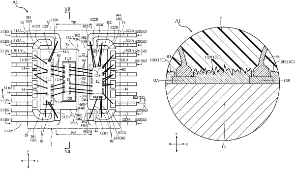
1. A semiconductor device comprising:
a first die pad that is arranged on one side of a first direction orthogonal to a thickness direction;
a second die pad that is arranged on the other side of the first direction with respect to the first die pad, is located away from the first die pad in the first direction, and has a potential that is relatively different from a potential of the first die pad;
a first semiconductor element that is mounted on the first die pad and forms a first circuit together with the first die pad;
a second semiconductor element that is mounted on the second die pad and forms a second circuit together with the second die pad;
an insulating element that is mounted on one of the first die pad and the second die pad, relays transmission and reception of signals between the first circuit and the second circuit, and insulates the first circuit and the second circuit from each other;
a plurality of first terminals that includes a portion located on the one side of the first direction with respect to the first die pad and is arranged along a second direction orthogonal to both the thickness direction and the first direction, at least one of the plurality of first terminals conducting to the first circuit;
a plurality of second terminals that includes a portion located on the other side of the first direction with respect to the second die pad and is arranged along the second direction, at least one of the plurality of second terminals conducting to the second circuit; and
a sealing resin that covers the first die pad, the second die pad, the first semiconductor element, the second semiconductor element, the insulating element, and a portion of each of the plurality of first terminals and the plurality of second terminals, and insulates the first die pad and the second die pad from each other,
wherein the sealing resin has a top surface facing a side where the first semiconductor element is located with respect to the first die pad in the thickness direction, a bottom surface facing an opposite side to the top surface in the thickness direction, and a first side surface located on the one side of the first direction and connected to the top surface and the bottom surface,
wherein the first side surface includes a first region connected to the top surface, a second region connected to the bottom surface, and a third region connected to the first region and the second region, the plurality of first terminals being exposed to the third region, and
wherein a surface roughness of each of the top surface, the bottom surface, the first region, and the second region is larger than a surface roughness of the third region.
|