| CPC H01L 23/293 (2013.01) [H01L 23/3157 (2013.01); H01L 23/34 (2013.01); H01L 29/1608 (2013.01); H01L 29/41775 (2013.01); H01L 29/7803 (2013.01); H01L 29/7813 (2013.01); H02M 7/53871 (2013.01)] | 19 Claims |

|
1. A semiconductor device comprising:
a semiconductor substrate made of a semiconductor having a higher linear expansion coefficient than silicon, the semiconductor substrate including a source region having a first conductivity type, a base region having a second conductivity type different from the first conductivity type, and a drift layer separated from the source region by the base region and having the first conductivity type, the semiconductor substrate having a main surface including a portion formed of the source region;
a gate dielectric film covering the base region of the semiconductor substrate;
a gate electrode facing the base region of the semiconductor substrate through the gate dielectric film;
a first electrode film electrically connected to the source region of the semiconductor substrate, and disposed over the main surface of the semiconductor substrate;
a second electrode film electrically connected to the gate electrode, and disposed over the main surface of the semiconductor substrate away from the first electrode film;
a third electrode film disposed over the main surface of the semiconductor substrate away from the first electrode film; and
a protective dielectric film disposed over the main surface of the semiconductor substrate, the main surface provided with the first electrode film, the second electrode film, and the third electrode film, the protective dielectric film covering only a portion of each of the first electrode film and the second electrode film and covering at least portion of the third electrode film, the protective dielectric film being made of a thermosetting resin, wherein
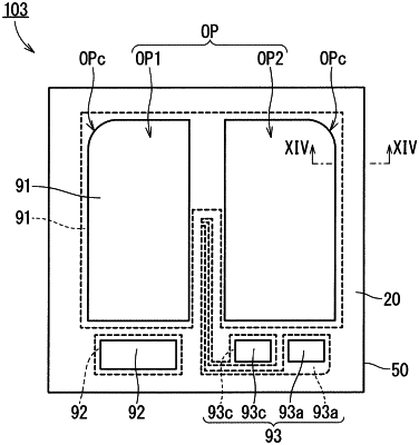
the main surface of the semiconductor substrate has a peripheral region and an inner region enclosed by the peripheral region, and the protective dielectric film has a peripheral portion covering the peripheral region and has a first inner portion covering at least portion of the third electrode film and crossing the inner region,
the semiconductor device further comprises at least one electrical element connected to the third electrode film, and covered with the first inner portion of the protective dielectric film,
the protective dielectric film has an opening so that the protective film covers less than half of the main surface of the semiconductor substrate,
the opening has an edge in plan view having a first corner portion on a corner side of the main surface, and the first corner portion is curved,
the edge of the opening has, in the plan view, a second corner portion formed with the peripheral region and the first inner portion of the protective dielectric film, and
the first corner portion is curved more gently than the second corner portion,
wherein the at least one electrical element is entirely covered with the first inner portion of the protective dielectric film in plan view and is located in the inner region closer to a center of the semiconductor device than an edge of the semiconductor device.
|