| CPC H01L 21/823814 (2013.01) [H01L 21/8221 (2013.01); H01L 21/823807 (2013.01); H01L 21/823871 (2013.01); H01L 21/823885 (2013.01); H01L 27/0688 (2013.01); H01L 27/092 (2013.01)] | 19 Claims |

|
1. A method of forming an electrical connection, the method comprising:
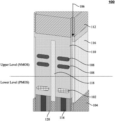
performing silicon epitaxial growth in a lower level of a complementary field effect transistor (CFET) structure to form at least one of a source and a drain in the lower level of the CFET structure;
forming two vertical dividers to create a vertical slot therebetween, wherein the two vertical dividers are adjacent to the at least one of the source and the drain;
adding a contact material to at least a portion of an exposed portion of the silicon epitaxial growth in the lower level, the exposed portion of the silicon epitaxial growth being located in the vertical slot of the CFET structure;
adding a conductive material within a vertical channel formed in the CFET structure, the conductive material being in contact with (i) the contact material added to the portion of the exposed portion of the silicon epitaxial growth in the lower level and (ii) a buried power rail (BPR) to form an electrical connection between the portion of the exposed portion of the silicon epitaxial growth and the BPR; and
etching back a portion of the added conductive material within the vertical channel,
wherein, during the adding of the contact material, an unexposed portion of the silicon epitaxial growth is located in the vertical slot and is covered by a blocking material, such that the contact material is only added to the exposed portion of the silicon epitaxial growth.
|