| CPC H01L 21/823807 (2013.01) [H01L 21/7806 (2013.01); H01L 21/823828 (2013.01); H01L 27/092 (2013.01)] | 11 Claims |

|
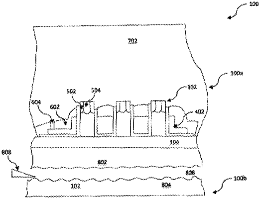
1. A method of forming an electronic device, comprising:
forming a plurality of channel structures over a first side of a semiconductor substrate, the plurality of channel structures substantially perpendicular to the first side of the semiconductor substrate;
forming gate dielectric regions over a portion of the plurality of channel structures and planar regions;
forming gate electrode regions over a portion of the gate dielectric regions;
forming source regions and body tie regions on the walls of the plurality of channel structures;
forming dielectric regions over the gate electrode regions to electrically isolate the gate electrode regions from the source regions;
forming a first metallic layer over the first side of the semiconductor substrate;
inducing stress within the semiconductor substrate by annealing and/or cooling the semiconductor substrate and the first metallic layer;
separating a first portion of the semiconductor substrate and the first metallic layer from a second portion of the semiconductor substrate;
forming backside metal regions over the first portion of the semiconductor substrate, the backside metal regions capable of being drain metal electrode contacts; and
etching portions of the first metallic layer to form gate metal electrode contacts and source metal electrode contacts.
|