| CPC H01L 21/7806 (2013.01) [H01L 21/0242 (2013.01); H01L 21/0254 (2013.01); H01L 21/02378 (2013.01); H01L 21/02381 (2013.01); H01L 21/02389 (2013.01); H01L 21/02609 (2013.01); H01L 29/045 (2013.01); H01L 29/2003 (2013.01); H01L 29/205 (2013.01); H01L 29/66462 (2013.01); H01L 29/7786 (2013.01)] | 17 Claims |

|
1. A manufacturing method for a transistor, comprising:
(i) growing crystals of a barrier layer and a channel layer made of a nitride semiconductor in a c-axis direction on a first substrate;
(ii) preparing a second substrate made of a semiconductor with no nitrogen contained;
(iii) bonding the second substrate to the barrier layer on the first substrate;
(iv) removing the first substrate, wherein the barrier layer and the channel layer remain on the second substrate;
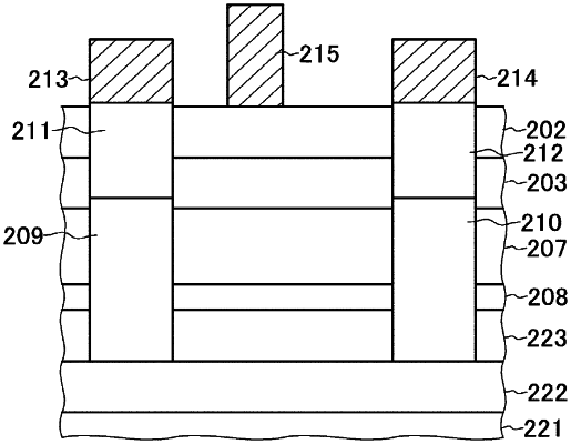
(v) forming, after the first substrate is removed, a first groove and a second groove in the barrier layer and the channel layer, the first groove and the second groove passing through the barrier layer and the channel layer with a region in which a gate electrode is to be formed interposed between the first groove and the second groove;
(vi) forming, in the first groove and the second groove, respectively, a source region and a drain region in contact with the channel layer by regrowing a semiconductor with no nitrogen contained in which impurities are injected from a side of a bottom surface of the first groove and from a side of a bottom surface of the second groove;
(vii) forming a source electrode to be ohmic-connected on the source region and forming a drain electrode to be ohmic-connected on the drain region; and
(viii) forming the gate electrode over the barrier layer and the channel layer between the source electrode and the drain electrode.
|