| CPC H01L 21/76895 (2013.01) [H01L 21/76805 (2013.01); H01L 21/76829 (2013.01); H01L 23/535 (2013.01); H10B 41/27 (2023.02); H10B 43/27 (2023.02)] | 28 Claims |

|
1. A method used in forming a memory array comprising strings of memory cells, comprising:
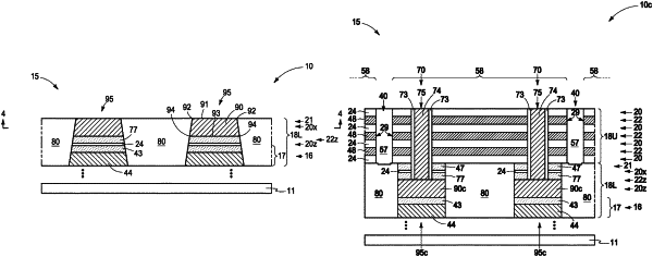
forming a lower portion of a stack comprising a through-array-via (TAV) region and an array region, the lower portion comprising a conductor tier comprising conductor material and multiple different composition materials directly above the conductor tier;
forming islands in the TAV region, individual of the islands comprising the conductor material of the conductor tier and the multiple different composition materials there-above, the individual islands comprising an etch-stop material, the etch-stop material comprising at least one of (a), (b), or (c), where:
(a): the individual islands having a top material that is the etch-stop material and that is of different composition from all material that is vertically between the etch-stop material and the conductor material;
(b): the top material of the individual islands being the etch-stop material and having its top surface in a vertical cross-section extending laterally-outward beyond two opposing laterally-outermost edges of a top surface of the material that is immediately directly below the top material; and
(c): a different composition from that of an upper portion of the conductor material and being in the conductor tier or being directly against the conductor material of the conductor tier;
forming an upper portion of the stack directly above the lower portion, the upper portion being formed in the TAV region above the islands and in the array region, the upper portion comprising vertically-alternating different composition first tiers and second tiers;
etching a TAV opening in the TAV region through the first tiers and the second tiers to stop on the etch-stop material of the individual islands; and
forming an operative TAV in the TAV opening that directly electrically couples with the conductor material in the conductor tier of the individual islands and forming strings of memory cells in the array region that directly electrically couple to the conductor material in the conductor tier.
|