| CPC H01L 21/76224 (2013.01) [H01L 23/3736 (2013.01); H01L 21/763 (2013.01); H01L 27/082 (2013.01); H01L 27/1203 (2013.01)] | 18 Claims |
|
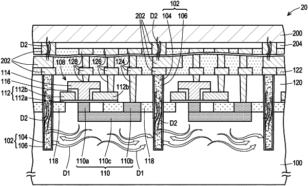
1. A semiconductor structure, comprising:
a substrate;
a deep trench isolation structure disposed in the substrate and not electrically connected to any device, wherein the deep trench isolation structure comprises:
a heat dissipation layer disposed in the substrate; and
a dielectric liner layer disposed between the heat dissipation layer and the substrate;
a heat sink disposed on the heat dissipation layer; and
an interconnect structure disposed between the heat sink and the heat dissipation layer, wherein the interconnect structure is in direct and physical contact with the heat sink and the heat dissipation layer.
|