| CPC H01L 21/743 (2013.01) [H01L 21/76805 (2013.01); H01L 23/5286 (2013.01); H01L 23/535 (2013.01); H01L 27/0886 (2013.01)] | 7 Claims |
|
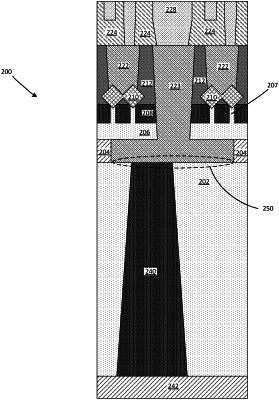
1. A semiconductor device comprising:
a first substrate;
a second substrate;
a SiGe layer provided between the first substrate and the second substrate;
a buried power rail (BPR) extending through the first substrate and the SiGe layer, a bottom portion of the BPR having portions extending laterally therefrom in the SiGe layer and having a width greater than a width of a top portion of the BPR; and
a nano though-silicon via formed in the second substrate in contact with the BPR,
wherein a width of the bottom portion of the BPR is greater than a width of the nano through-silicon via in contact therewith, and
wherein a thickness of the bottom portion of the BPR is less than a width of the top portion of the BPR.
|