| CPC H01J 37/153 (2013.01) [H01J 37/14 (2013.01); H01J 37/147 (2013.01); H01J 37/28 (2013.01); H01J 2237/141 (2013.01); H01J 2237/1534 (2013.01)] | 14 Claims |

|
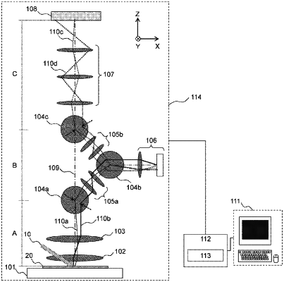
1. An electron beam application apparatus, comprising,
a sample stage on which a sample is to be placed;
an electron optical system which includes an objective lens for forming an electronic image by electrons emitted from the sample and which has an optical axis perpendicular to a sample mounting surface of the sample stage; and
a camera which images the electronic image; wherein
the electron optical system includes
a mirror aberration corrector disposed perpendicular to the optical axis;
a plurality of magnetic field sectors by which an orbit of electrons passing through the objective lens is deviated from the optical axis to make the electrons incident on the mirror aberration corrector, and the orbit of the electrons emitted from the mirror aberration corrector is returned to the optical axis; and
a doublet lens disposed between adjacent magnetic field sectors along the orbit of the electrons,
each of the plurality of magnetic field sectors has a same deflection angle for deflecting the orbit of the electrons, and
the doublet lens is disposed such that an object plane and an image plane thereof are respectively central planes of the adjacent magnetic field sectors along the orbit of the electrons.
|