| CPC G11C 29/44 (2013.01) [G11C 29/4401 (2013.01); G11C 29/76 (2013.01); H01L 25/18 (2013.01); H10B 12/50 (2023.02); G11C 5/04 (2013.01); G11C 2029/1208 (2013.01); H01L 27/0688 (2013.01); H01L 27/105 (2013.01); H01L 2924/0002 (2013.01); Y10T 29/49002 (2015.01)] | 20 Claims |

|
1. A memory device, comprising:
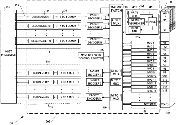
a stack of multiple memory die electrically connected with one another by through wafer interconnects extending through the stack of multiple memory die, the stack of multiple memory die comprising multiple partitions respectively including one or more arrays from each of two or more memory die of the stack of multiple memory die, the multiple partitions comprising multiple first partitions established according to a first memory map; and
control logic operably coupled to the stack of multiple memory die, the control logic operable to monitor portions of the stack of multiple memory die to collect error data indicating defective portions within one or more of the multiple partitions, and to remove a defective portion from one or more of the multiple partitions.
|