| CPC G11C 13/0033 (2013.01) [G11C 13/0004 (2013.01); G11C 13/004 (2013.01); G11C 13/0038 (2013.01); G11C 13/0069 (2013.01); G11C 29/021 (2013.01); G11C 29/12005 (2013.01)] | 17 Claims |

|
1. A memory device, comprising:
a plurality of memory cells, comprising:
a first group of memory cells; and
a second group of memory cells programmed to a predefined logic state of the at least two logic states; and
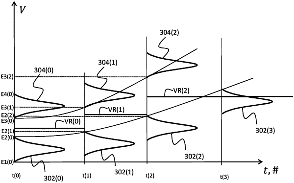
a memory controller coupled to the plurality of memory cells and configured to carry out a recovery voltage setting operation to set the recovery voltage, the recovery voltage setting operation comprising:
applying a test voltage corresponding to a reading voltage applied to at least one selected memory cell of the first group of memory cells to the memory cells of the second group to assess a logic state thereof;
biasing a corresponding word line to a word line selection voltage lower than the reading voltage;
responsive to the logic state of at least one memory cell of the second group assessed with the test voltage being different from the predefined logic state:
increasing the value of the test voltage;
repeating application of the test voltage to the memory cells of the second group to assess the logic state thereof using the increased value of the test voltage; and
responsive to the logic state of all the memory cells of the second group assessed with the test voltage being equal to the predefined logic state, setting the recovery voltage according to the test voltage used in a last application of the test voltage to the memory cells of the second group to assess the logic state thereof that has been carried out.
|