| CPC G11C 11/4093 (2013.01) [G06F 3/0656 (2013.01); G06F 13/1673 (2013.01); G06F 13/28 (2013.01); G11C 7/08 (2013.01); G11C 7/1039 (2013.01); G11C 11/4087 (2013.01); G11C 11/4091 (2013.01); G11C 11/4096 (2013.01); G16B 30/00 (2019.02); G16B 50/10 (2019.02); H01L 21/78 (2013.01); H01L 22/12 (2013.01); H01L 24/08 (2013.01); H01L 24/48 (2013.01); H01L 24/80 (2013.01); H01L 25/0652 (2013.01); H01L 25/0657 (2013.01); H01L 25/18 (2013.01); H01L 25/50 (2013.01); G06F 2213/28 (2013.01); H01L 24/16 (2013.01); H01L 2224/0801 (2013.01); H01L 2224/08145 (2013.01); H01L 2224/1601 (2013.01); H01L 2224/16221 (2013.01); H01L 2224/48091 (2013.01); H01L 2224/48145 (2013.01); H01L 2224/48221 (2013.01); H01L 2224/80895 (2013.01); H01L 2224/80896 (2013.01); H01L 2225/06517 (2013.01); H01L 2225/06524 (2013.01); H01L 2225/06527 (2013.01); H01L 2225/06541 (2013.01); H01L 2225/06565 (2013.01); H01L 2225/06589 (2013.01); H01L 2924/1431 (2013.01); H01L 2924/1436 (2013.01); H01L 2924/14335 (2013.01)] | 20 Claims |
|
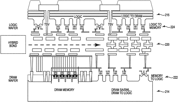
18. An apparatus, comprising:
a memory die, comprising:
a memory array;
a plurality of local input/output lines (LIOs) coupled to the memory array; and
a global input/output line coupled to the plurality of LIOs and to a host interface;
a logic die bonded to the memory die via a wafer-on-wafer bonding process, the logic die comprising logic circuitry configured to:
receive signals indicative of data from the memory die and through a wafer-on-wafter bond to the plurality of LIOs, wherein the data comprises genetic sequence data;
perform genome annotation logic operations to attach biological information to the genetic sequence data; and
generate an annotated genetic sequence based on the genome annotation logic operations.
|