| CPC G11C 11/4091 (2013.01) [G11C 7/08 (2013.01); G11C 7/1006 (2013.01); G11C 11/4076 (2013.01); G06F 3/068 (2013.01); G06F 3/0611 (2013.01); G06F 3/0659 (2013.01); G11C 7/1048 (2013.01); G11C 11/4093 (2013.01); G11C 11/4096 (2013.01)] | 20 Claims |

|
1. A system, comprising:
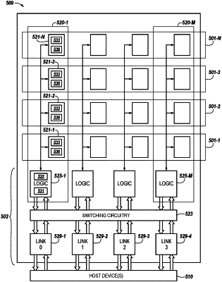
a plurality of processing in memory (PIM) devices to perform PIM operations, the plurality of PIM devices comprising:
a first PIM device comprising:
a first plurality of banks, each bank of the first plurality of banks comprising a respective array of memory cells and respective sensing circuitry, wherein at least two banks of the first plurality of banks are on different memory components of a plurality of memory components stacked with a logic component;
a first plurality of timing circuitries respectively coupled to the first plurality of banks; and
a first control logic on the logic component coupled to the first plurality of banks and the first plurality of timing circuitries; and
a second PIM device comprising:
a second plurality of banks, each bank of the second plurality of banks comprising a respective array of memory cells and respective sensing circuitry, wherein at least two banks of the second plurality of banks are on different memory components of the plurality of memory components;
a second plurality of timing circuitries respectively coupled to the second plurality of banks; and
a second control logic on the logic component coupled to the second plurality of banks and the second plurality of timing circuitries; and
wherein the plurality of PIM devices further comprises switching circuitry configured to:
route memory array requests received from a host; and
route PIM requests received from the host to perform a logical operation.
|