| CPC G09G 3/3233 (2013.01) [H10K 59/1315 (2023.02); G09G 2300/0408 (2013.01); G09G 2300/0426 (2013.01); G09G 2300/0452 (2013.01); G09G 2300/0819 (2013.01); G09G 2300/0842 (2013.01); G09G 2300/0861 (2013.01); G09G 2310/0272 (2013.01); G09G 2310/08 (2013.01); G09G 2320/043 (2013.01); G09G 2330/026 (2013.01)] | 18 Claims |

|
1. A display substrate, comprising:
a base substrate; and
a plurality of sub-pixels, located on the base substrate and arranged in an array,
wherein each of the plurality of sub-pixels comprises a pixel circuit, and the pixel circuit is configured to drive a light-emitting element corresponding to the each of the plurality of sub-pixels to emit light;
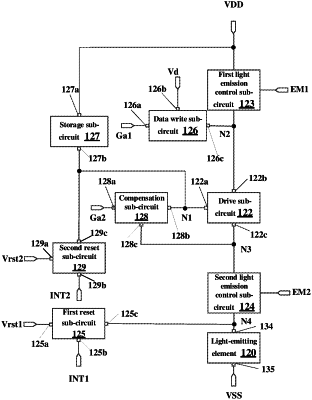
each of the plurality of pixel circuits comprises a drive sub-circuit, a data write sub-circuit, a compensation sub-circuit, a storage sub-circuit, and a first reset sub-circuit;
the drive sub-circuit comprises a control terminal, a first terminal, and a second terminal, and the drive sub-circuit is configured to be connected with the light-emitting element and control a drive current flowing through the light-emitting element;
the data write sub-circuit is connected with the first terminal of the drive sub-circuit and is configured to write a data signal into the first terminal of the drive sub-circuit in response to a first scanning signal;
the compensation sub-circuit comprises a control terminal, a first terminal and a second terminal, and the control terminal of the compensation sub-circuit is configured to receive a second scanning signal, the first terminal and the second terminal of the compensation sub-circuit are respectively electrically connected with the control terminal and the second terminal of the drive sub-circuit, and the compensation sub-circuit is configured to compensate a threshold value of the drive sub-circuit in response to the second scanning signal;
the storage sub-circuit comprises a first terminal and a second terminal, the first terminal of the storage sub-circuit is configured to receive a first power supply voltage, and the second terminal of the storage sub-circuit is electrically connected with the control terminal of the drive sub-circuit;
the first reset sub-circuit comprises a control terminal, a first terminal, and a second terminal, the control terminal of the first reset sub-circuit is configured to receive a first reset control voltage, the first terminal of the first reset sub-circuit is configured to receive a first reset voltage, and the second terminal of the first reset sub-circuit is configured to be connected with the light-emitting element;
the first reset sub-circuit is configured to apply the first reset voltage to the light-emitting element to reversely bias the light-emitting element in response to the first reset control voltage; and
the plurality of sub-pixels comprise a first sub-pixel, the display substrate further comprises a first reset voltage terminal, and the first reset voltage terminal is configured to be connected with a first terminal of the first reset sub-circuit of the first sub-pixel to provide the first reset voltage to the first sub-pixel;
the plurality of sub-pixels are arranged in a plurality of pixel rows along a first direction and a plurality of pixel columns along a second direction, and the display substrate further comprises a first reset voltage line extended along the first direction, and the first reset voltage line is electrically connected with the first reset voltage terminal and the first terminal of the first reset sub-circuit respectively to provide the first reset voltage for the plurality of sub-pixels;
the plurality of sub-pixels further comprises a second sub-pixel, and the first sub-pixel and the second sub-pixel correspond to light-emitting elements emitting different colors;
the display substrate further comprises a second reset voltage terminal, and the second reset voltage terminal is configured to be connected with the first terminal of the first reset sub-circuit of the second sub-pixel to provide the first reset voltage to the second sub-pixel; and
the first reset voltage output by the first reset voltage terminal is different from the first reset voltage output by the second reset voltage terminal.
|