| CPC G09G 3/32 (2013.01) [G09G 2300/0842 (2013.01); G09G 2310/0267 (2013.01); G09G 2310/0275 (2013.01); G09G 2310/0278 (2013.01); G09G 2310/08 (2013.01)] | 20 Claims |
|
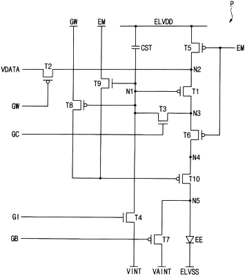
1. A pixel circuit comprising:
a light-emitting element;
a write transistor which writes a data voltage;
a driving transistor which generates a driving current based on the data voltage and applies the driving current to the light-emitting element;
a first initialization transistor which applies a first initialization voltage to a control electrode of the driving transistor;
a blocking transistor disposed between the light-emitting element and the driving transistor;
a first blocking control transistor including:
a control electrode connected to the control electrode of the driving transistor;
a first electrode which receives a first signal; and
a second electrode connected to a control electrode of the blocking transistor; and
a second blocking control transistor including a control electrode connected to the control electrode of the driving transistor, a first electrode which receives a second signal, and a second electrode connected to the control electrode of the blocking transistor.
|