| CPC G06F 30/398 (2020.01) [G06F 30/392 (2020.01)] | 20 Claims |
|
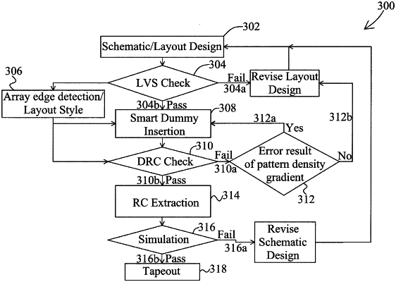
1. A system for manufacturing a semiconductor device comprising:
an array edge detection tool configured to determine whether a layout design of the semiconductor device includes a plurality of active cells or at least one dummy cell;
a layout style determination tool configured to detect whether the plurality of active cells have a distributed layout style;
a layout versus schematic (LVS) tool configured to compare a schematic design of the semiconductor device to the layout design of the semiconductor device; and
a dummy insertion tool configured to revise the layout design of the semiconductor device based on the layout design and the schematic design by revising an area of the at least one dummy cell when the array edge detection tool determines that the layout design includes the at least one dummy cell, or inserting the at least one dummy cell between the plurality of active cells and an outside edge of the semiconductor device when the array edge detection tool determines that the layout design does not include the at least one dummy cell.
|