| CPC G06F 3/0655 (2013.01) [G06F 3/0604 (2013.01); G06F 3/0679 (2013.01)] | 20 Claims |

|
1. A method comprising:
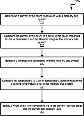
determining a current cycle count associated with a memory sub-system;
measuring a temperature associated with the memory sub-system;
identifying, in a data structure, a current lifecycle stage corresponding to the current cycle count;
in response to identifying the current lifecycle stage, identifying, in the data structure, a threshold range corresponding to the temperature associated with the memory sub-system;
selecting, from the data structure, a write-to-read (W2R) delay time corresponding to the current lifecycle stage and the threshold range associated with the temperature associated with the memory sub-system; and
executing, by a processing device, a read operation associated with a memory unit of the memory sub-system, following a period of at least the W2R delay time from a time of an execution of a write operation associated with the memory unit.
|