| CPC G06F 3/0443 (2019.05) [G06F 3/0446 (2019.05)] | 20 Claims |

|
1. An organic light-emitting diode (OLED) display comprising:
a substrate;
a buffer layer on the substrate;
a plurality of thin film transistors (TFT) on the buffer layer, each of the thin film transistors comprising an active layer and a gate electrode;
a plurality of pixels including a plurality of light emitting layers between a plurality of lower electrodes and an upper electrode on the substrate;
a thin film encapsulation layer on the upper electrode;
a pixel defining layer on the substrate, the pixel defining layer partially exposing the lower electrodes;
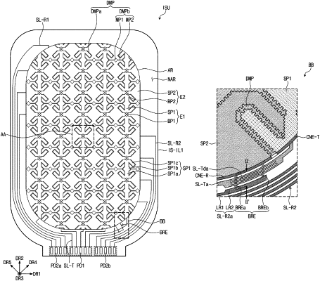
a touch sensor unit comprising a plurality of first electrodes and a plurality of second electrodes spaced apart from the first electrodes; and
a line comprising a first line connected to one of the first electrodes and a second line connected to one of the second electrodes,
wherein:
the second line includes a main line and a sub-line electrically connected to the main line and one of the second electrodes;
the sub-line crosses the first line disposed between the second electrode and the main line in a plan view and is insulated from the first line; and
an insulating layer is disposed between the sub-line and first line.
|