| CPC G02F 1/2257 (2013.01) [G02F 1/0147 (2013.01); G02F 1/025 (2013.01); G02F 1/3135 (2021.01); G02F 2203/15 (2013.01)] | 16 Claims |

|
1. A hybrid photonic ring modulator for modulating light at a target operating wavelength, the photonic ring modulator comprising:
a silicon bus waveguide formed in a silicon device layer of a silicon-on-insulator (SOI) substrate; and
a ring resonator structure formed above the silicon device layer, the ring resonator structure comprising a p-i-n diode structure of compound semiconductor material and associated electrodes, an active region of the p-i-n diode structure forming a ring waveguide laterally overlapping with the silicon bus waveguide, the ring waveguide and the silicon bus waveguide together forming a vertical directional coupler in an overlap region;
a heater placed above the silicon device layer near the p-i-n diode structure;
electronic driver circuitry electrically connected to the electrodes to apply a voltage across the p-i-n-diode structure, the voltage including a reverse bias voltage and a radio-frequency (RF) voltage swing; and
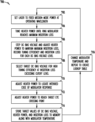
memory storing a target value of the reverse bias voltage and a target value of a power of the heater,
wherein the target value of the reverse bias voltage maximizes a tuning efficiency of shifting, by a change in the applied voltage, a spectral location of a modulator response of the photonic ring modulator, subject to exceeding a specified loss cutoff level for a maximum modulator insertion loss at a resonance wavelength of the modulator response, and
wherein the target value of the power of the heater optimizes an offset between the resonance wavelength of the modulator response at the target value of the reverse bias voltage and the target operating wavelength to achieve a target insertion loss at the target operating wavelength.
|