| CPC G01R 31/2863 (2013.01) [G01R 31/2875 (2013.01); H01R 12/88 (2013.01); H01R 33/88 (2013.01); H01R 33/97 (2013.01); H01R 33/74 (2013.01); H01R 2201/20 (2013.01)] | 21 Claims |

|
1. A burn-in board for burn-in testing of devices, the device comprising:
a printed circuit board (PCB);
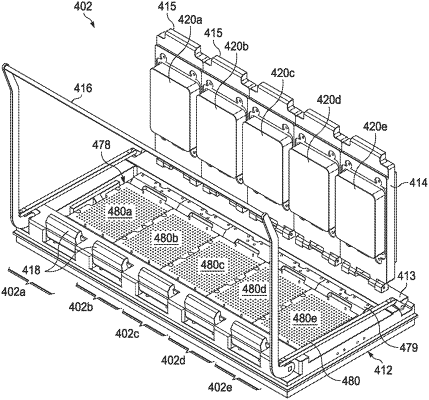
a strip socket mounted to the PCB, the strip socket including:
a socket base configured to receive a device strip including an array of devices mounted on a device strip substrate;
a socket lid;
at least one heating block associated with the socket lid;
wherein the socket lid is movable between (a) an open position allowing the device strip to be mounted on the socket base and (b) a closed position in which the mounted device strip is arranged between the socket lid and socket base; and
an array of conductive contacts, each configured to contact a respective device in the array of devices,
heating control circuitry configured to control the at least one heating block to provide heat to the device strip; and
burn-in test circuitry connected to the conductive contacts for communicating input test signals to individual devices of the array of devices on the device strip and output test signals from the individual devices.
|