| CPC G01J 1/44 (2013.01) [G01J 1/0271 (2013.01); G01J 1/0459 (2013.01); H01L 31/02016 (2013.01); G01J 2001/446 (2013.01); G01J 2001/4413 (2013.01)] | 19 Claims |

|
1. An optical sensor, comprising:
a first photodetector configured to be reverse biased at a first voltage exceeding a breakdown voltage of the first photodetector by a first excess bias voltage;
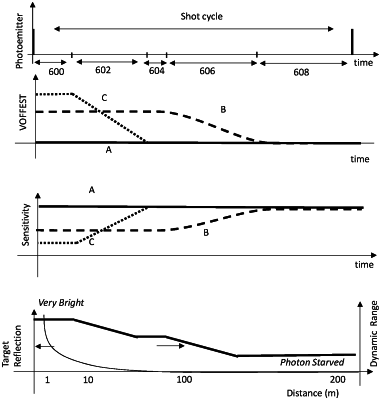
a second photodetector configured to be reverse biased at a second voltage exceeding a breakdown voltage of the second photodetector by a second excess bias voltage different from the first excess bias voltage, the second excess bias voltage being varied during a shot cycle of a photoemitter; and
a third photodetector configured to be reverse biased at a third voltage exceeding a breakdown voltage of the third photodetector by a third excess bias voltage, the third excess bias voltage being different from the first excess bias voltage and the second excess bias voltage, the third excess bias voltage being varied during the shot cycle of the photoemitter, wherein the second excess bias voltage is varied from a first value to a second value during a first portion of the shot cycle of the photoemitter, and the third excess bias voltage is varied from a third value to a fourth value during a second portion of the shot cycle of the photoemitter.
|