| CPC B81C 1/0015 (2013.01) [B81C 2201/0132 (2013.01); B81C 2201/0133 (2013.01); G02B 26/103 (2013.01)] | 17 Claims |

|
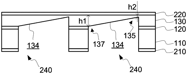
10. A semiconductor substrate comprising:
a first semiconductor layer;
a first dielectric layer coupled to the first semiconductor layer;
a second semiconductor layer coupled to the first dielectric layer, wherein the second semiconductor layer comprises:
a base portion substantially aligned with the first dielectric layer; and
a cantilever portion protruding from an end of the first dielectric layer, wherein the cantilever portion comprises a tapered surface tapering from a bottom surface of the second semiconductor layer toward a top surface of the second semiconductor layer;
a second dielectric layer coupled to the second semiconductor layer; and
a third semiconductor layer coupled to the second dielectric layer.
|